Laser Nanocrystallization of Si for solar applications.
In this work we are investigating the Nd:YAG laser annealing for the partial crystallization of an amorphous silicon layer,
in order to create tandem solar cell panels. In the initial structure, an a-Si:H thin film has been deposited upon a ZnO/Glass substrate using PECVD.
Our aim is an alternative formation of the μc-Si thin film upon the a-Si:H layer by crystallizing the upper part of the later, instead of using the conventional two step PECVD deposition of each film separately.
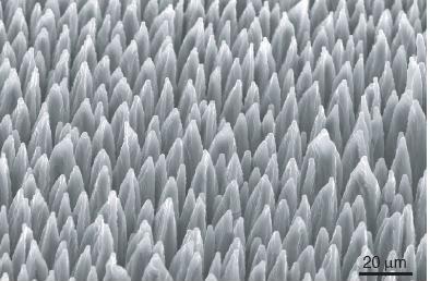
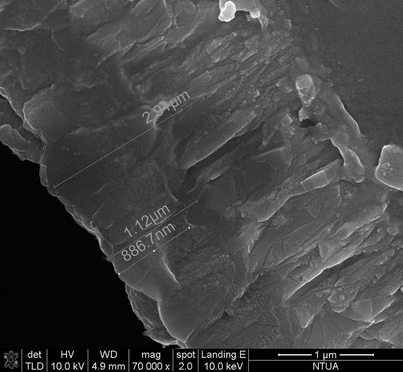
As the overall structure is consisted from three separate layers, prior to annealing we have performed a complete morphological characterization, including SEM, XRD, AFM, absorptivity and RAMAN spectroscopy on each layer,
in order to investigate their properties and morphology.
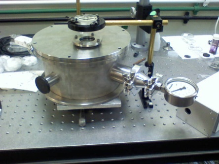
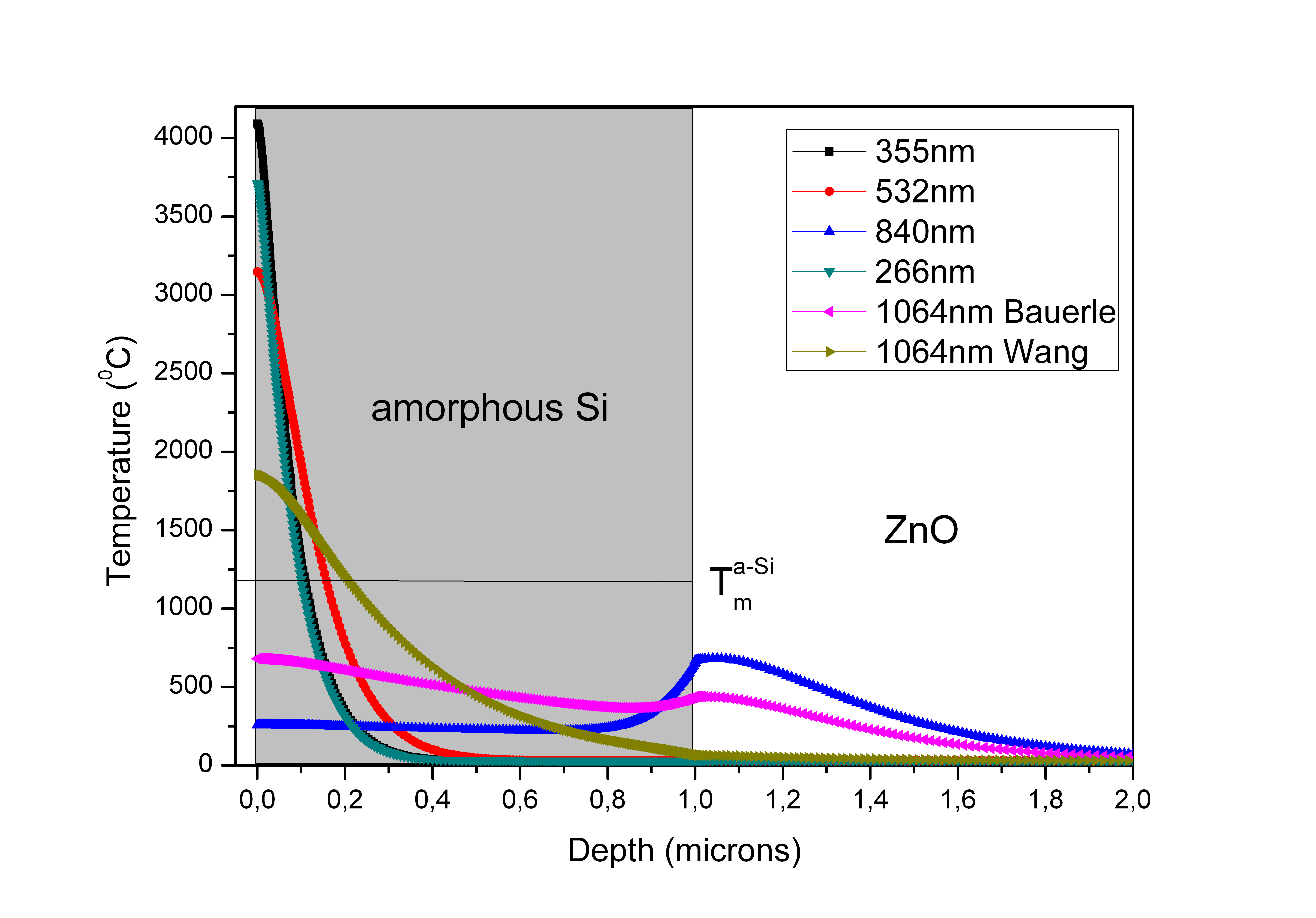
A Nd:YAG laser (FWHM=6 ns, energy ranging from 25 to 80 mJ) with air as an ambient medium has been used at two different wavelengths (532 and 1064 nm), in order to determine the optimum annealing conditions for the realization of the partial crystallization of a-Si layer. The laser experimental work is combined with simulation of the annealing effect, in terms of temperature distribution evolution, using the Synopsys Sentaurus Process TCAD software, so as to predetermine the optimum annealing conditions at each laser wavelength. In both cases irradiation takes place in the sub-melt regime, so as to avoid significant diffusion occurrence on the p and n doped layers within the structure. Annealed samples are subsequently characterized by means of SEM, XRD and RAMAN in order to investigate the effect of the irradiation on the crystallization of a part of a-Si layer, at the desired depth.
People
Ioannis Kalpyris, PhD student, NTUA
Ioanna Zergioti, Assis. Professor, NTUA